275nm UVC-LED 4040mil2芯片
275nm UVC-LED 4040mil2芯片
275nm UVC-LED 4040mil2芯片
- 产品详情
- 产品参数
275nm UVC-LED 4040mil2芯片
特性: Features
(1)亮度高 High luminous intensity.
(2)可应用于消毒 Used for sterilization
(3)高可靠性,长寿命 High reliability.
(4)百分百全测 100% Probing test.
(5)散热性好 Good heat dissipation
物理参数: Characteristics
1. 尺寸 Size
(1)芯片尺寸 Chip size: 40mil × 40mil (1018±25μm × 1018±25μm)
(2)芯片厚度 Chip thickness: 15.7mil (400±20μm)
(3)P电极 bonding pad: 32.8mil ×14.0mil (834±20μm × 357±20μm)
N电极 bonding pad: 32.8mil ×14.0mil (834±20μm × 357±20μm)
(4)P/N间距 P/N spacing: 5.9mil (150±20μm)
2. 金属电极 Metallization: P/N为金/锡电极 Au/Sn alloy
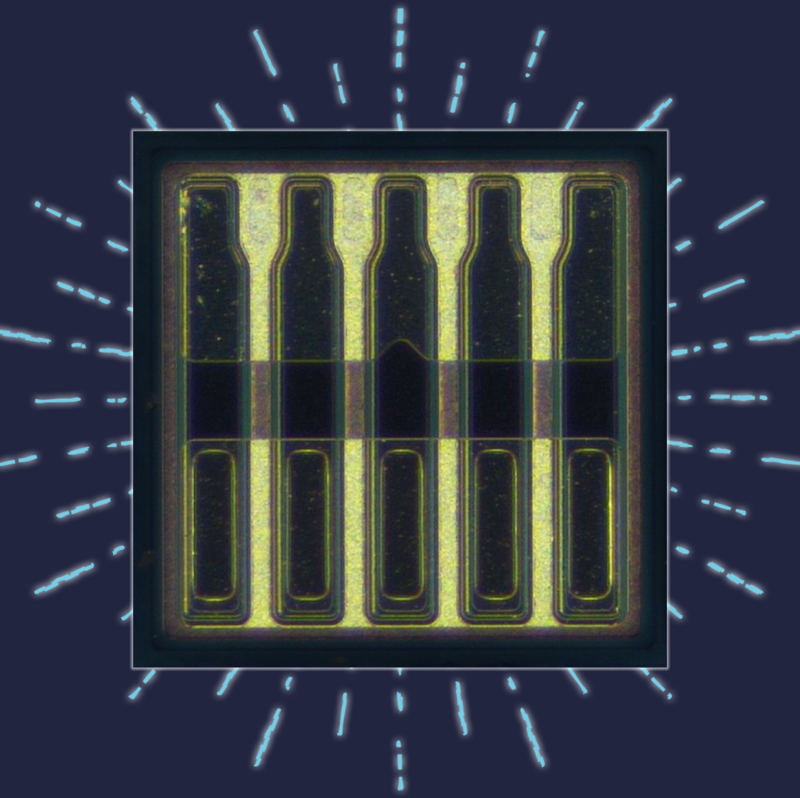
3. 结构 Structure: 参考右图 refer to the right figure.

25℃时光电特性: Electro-optical characteristic at 25℃
(测试参数) Test parameter | (测试条件) Test Condition | (最小值) Min | (典型值) Typ | (最大值) Max | (单位) Unit |
峰值波长 peak wavelength(Wp) | 350mA | 270 | 275 | 280 | nm |
输出光功率 Output power(Po) | 350mA | 50 | 75 | 100 | mW |
正向电压 Forward voltage(Vf) | 350mA | 5 | 5.7 | 6.5 | V |
反向电流 Reverse current(Ir) | -5V | 0 | — | 0.1 | μA |
备注 Notes:
1. 波长分档为5nm,然而我们也欢迎客户的其他要求 。
Basically, wavelength span is 5 nm, however, customers’special requirements
are also welcome.
2. 光功率分档为 5mW,然而我们也欢迎客户的其他要求。
Basically, Luminous power span is 5mW, however, customers’special requirements
are also welcome.
3. 电压分档为0.5V,然而我们也欢迎客户的其他要求。
Basically, Forward voltage span is 0.5V, however, customers’special requirements
are also welcome.
光电特性曲线: Electro-optical characteristic curve
正向电压 v.s. 正向电流 电光转换效率 v.s. 正向电流
Forward voltage v.s. Forward current Wall-plug efficiency v.s. Forward current
输出光功率 v.s. 正向电流 外量子效率 v.s. 正向电流
Light Output Power v.s. Forward current External quantum efficiency v.s. Forward current
归一化发光强度 v.s 发光波长 发光波长 v.s. 正向电流
Normalized Intensity v.s. Wavelength Wavelength v.s. Forward current
备注 Note:
上述测试数据源自中紫半导体科技,视抽样情况的不同,实际曲线将会存在一定差别。
The above test data are derived from SinoVio Semiconductor Technol. (Dongguan) Co. Ltd., and the actual curve will vary to some extent depending on the sampling situation.
绝对最大范围: Absolute Maximum Ratings
(参数) Parameter | (符号) Symbol | (条件) Condition | (范围) Rating | (单位) Unit |
(正向直流电流) Forward DC current | If | Ta=25℃ | ≤500 | mA |
(反向电压) Reverse voltage | Vr | Ta=25℃ | ≤10 | V |
(结温) Junction temperature | Tj | — | ≤80 | ℃ |
(封装加热温度) Temperature during packaging | — | — | 280 (<10sec) | ℃ |
(储存温度) Storage temperature | Tstg | 储存 chip-on- tape/storage | -40 ~ 85 | ℃ |
运输 chip-on- tape/transportation | -20 ~ 65 | ℃ |
备注 Note:
以上最大范围是通过无树脂涂层的印刷电路板所决定的,其与封装形式具高度相关性。施加大于最大范围如正向电流及结温等均会对LED产生危害。
Maximum ratings are package dependent. The above maximum ratings were determined using a Printed Circuit Board (PCB) without an encapsulant. Stresses in excess of the absolute maximum ratings such as forward current and junction temperature may cause damage to the LED.