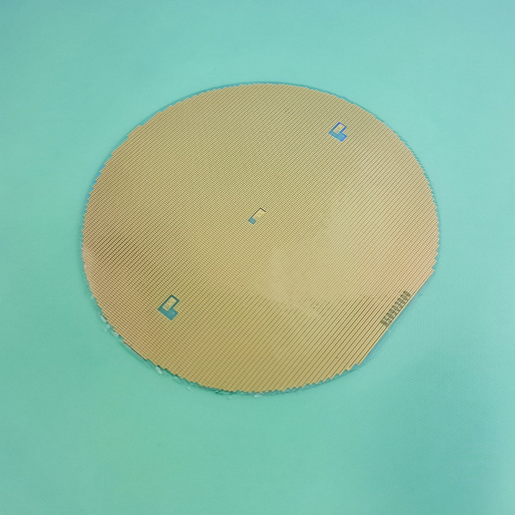
UVC-LED Chip
UVC-LED Chip
UVC-LED Chip
- Detail
- Parameters
Features:
(1) High luminous intensity
(2) Used for sterilization
(3) High reliability
(4) 100% Probing test
(5) Excellent heat dissipation
Characteristics:
1. Size:
(1) Chip size: 12mil × 20mil (305±25 µm × 506±25 µm)
(2) Chip thickness: 13.2mil (335±15µm)
(3) P type bonding pad: 4.7mil × 8.1mil (120±15μm × 205±15μm)
N type bonding pad: 6.5mil × 10.6mil (166±15μm × 270±15μm)
(4) P/N spacing:5.9mil (150±15μm)
2. Electrode Metallization: Au/Sn alloy
3. Structure:

Electro-optical characteristic at 25℃:
Parameters | Conditions | Min. | Typ. | Max. | Unit |
Peak wavelength | 40 mA | 270 | 275 | 280 | nm |
Luminous power (P0) | 40 mA | 4 | 6 | 8 | mW |
Forward voltage (VF1) | 40 mA | 5 | 6 | 7 | V |
Forward voltage (VF4) | 1 µA | 3 | - | 4.5 | V |
Reverse current (Ir) | -5 V | 0 | - | 0.1 | µA |
Forward Current vs. Forward Voltage: